II. Full Custom IC Design Using the Generic 0.13 μm Process
Table of Contents
Introduction
In this tutorial we will manually create the polygons which specifies transistor layouts and their interconnections. This process will help you understand IC layout (e.g., how to make and connect transistors to form an integrated circuit). A static CMOS inverter will be translated into a NWELL and PWELL generic 0.13 micron technology.
Prepare your Workspace
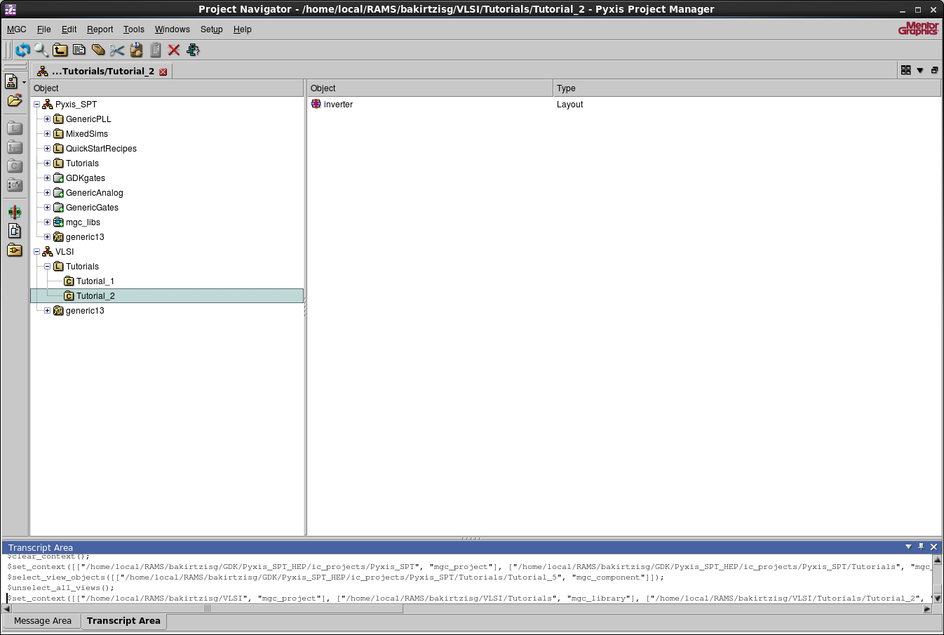
In the Pyxis Project Navigator open your project located in your home
folder. Then, add another cell to your project named Tutorial_2 and
create a layout called inverter.
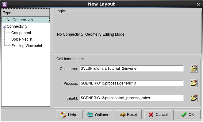
Pyxis Layout will open automatically. Be sure that No Connectivity is chosen and
that the process used is generic13.
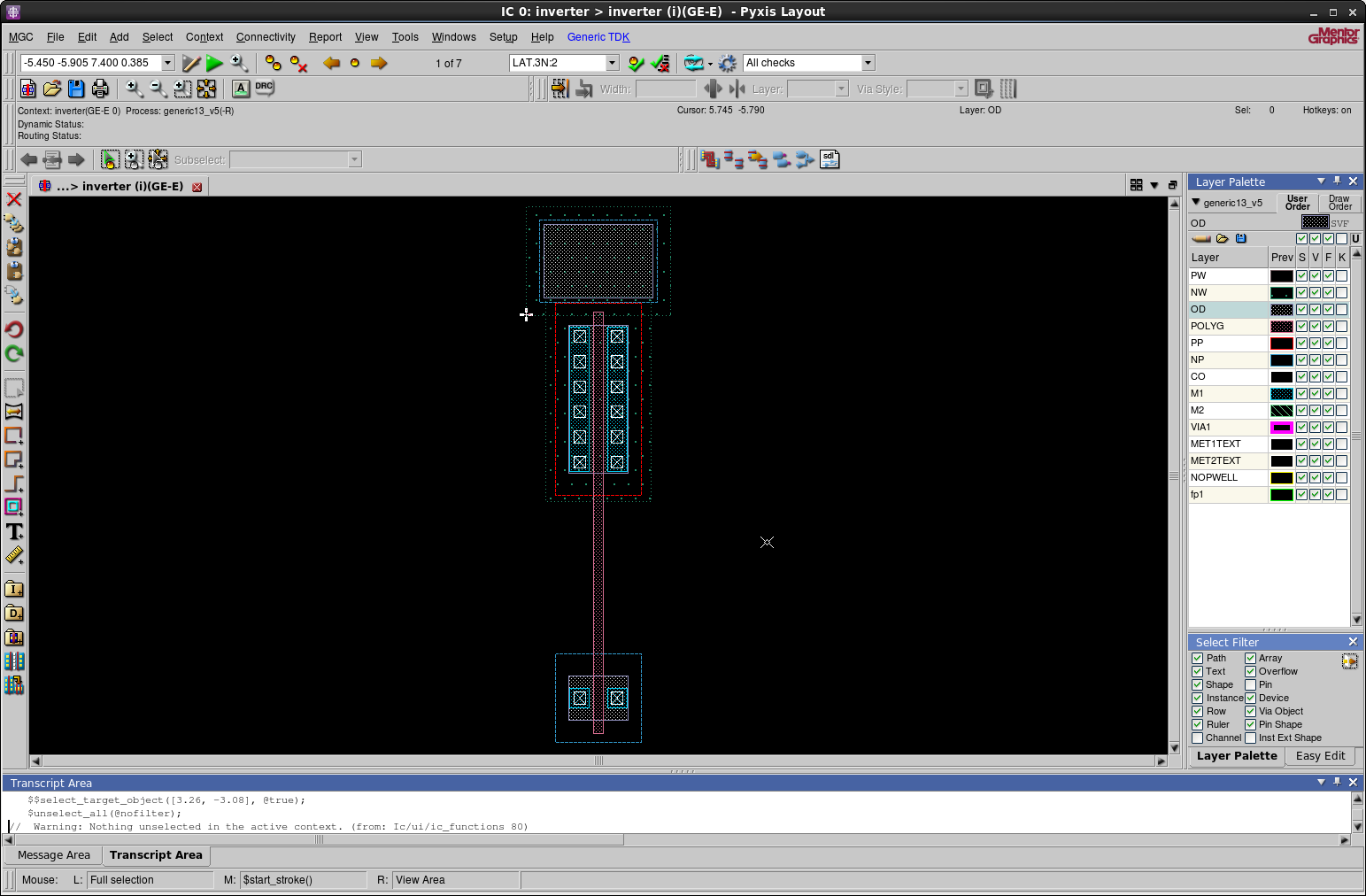
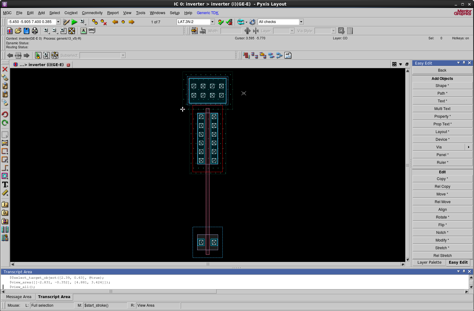
Laying polygons for the inverter
Creating the PMOS transistor
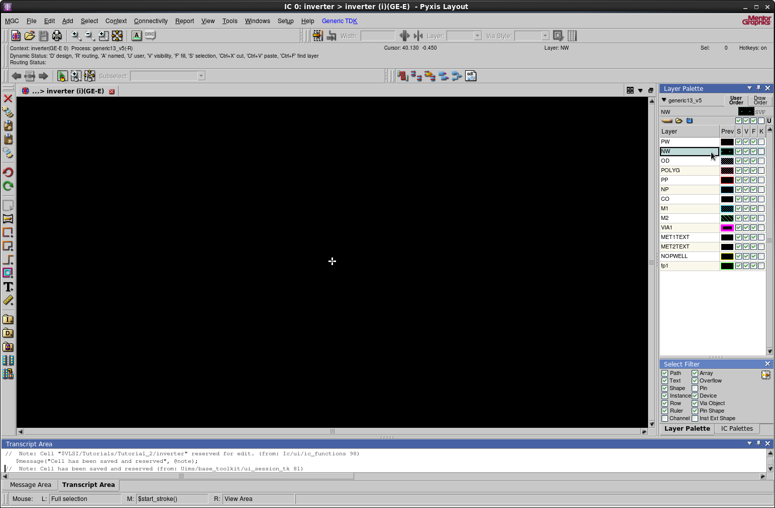
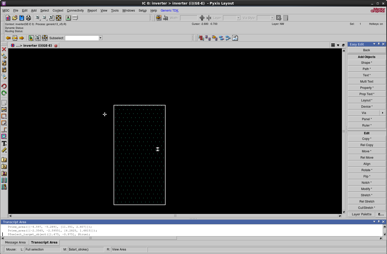
Navigate to Layer Palette and choose NW.
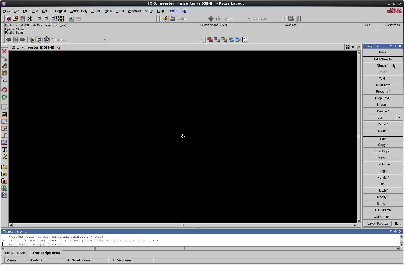
Navigate to IC Palettes > Easy Edit and choose Shape.
Make a shape anywhere in your sheet. Press ESC and then select the
object. Access its properties by pressing q. Change the width, height,
origin x, and origin y to the ones specified below.
| Width | 1.43 |
| Height | 2.78 |
| Origin X | 0.26 |
| Origin Y | -2.52 |
Realize that the Origin X and Origin Y are relative. The importance lies in how these blocks are spaced in the final layout. Therefore, you could have very different origins for your polygons and reach the same result.
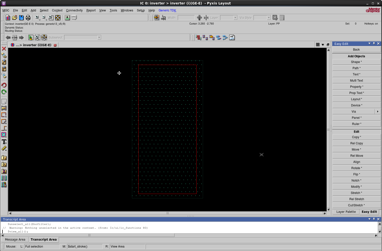
Add another polygon but of PP type and change the properties as
shown in the table below. It is advised that you
don't draw it on top of the already existing polygon because it doesn't
always work correctly. Instead draw your polygon away from the other shape
and change the origins from the properties.
| Width | 1.17 |
| Height | 2.6 |
| Origin X | 0.39 |
| Origin Y | -2.43 |
Similarly, we will lay the rest of the polygons that make the PMOS transistor.
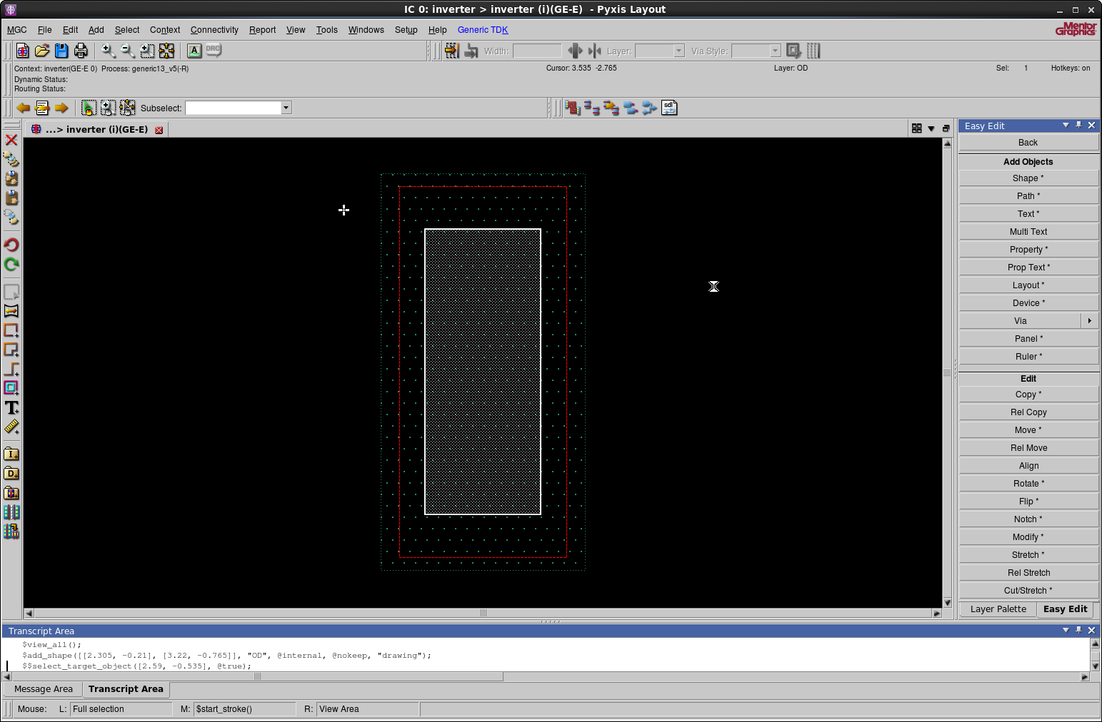
| Type | OD |
| Width | 0.81 |
| Height | 2 |
| Origin X | 0.57 |
| Origin Y | -2.13 |
| Type | M1 |
| Width | 0.26 |
| Height | 1.96 |
| Origin X | 0.59 |
| Origin Y | -2.11 |
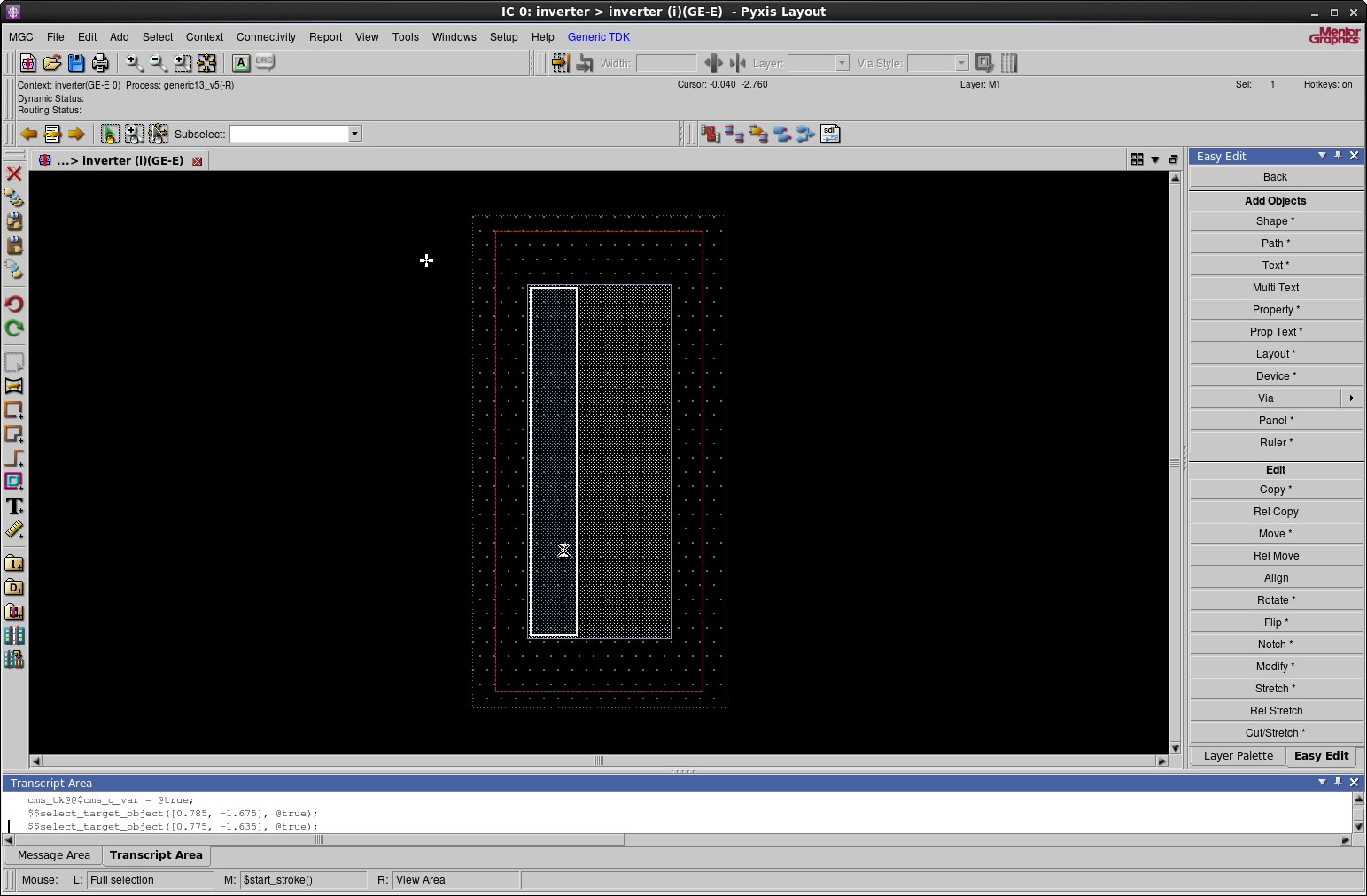
Press ESC and select the above shape. Then navigate to Easy Edit > Edit
> Rel Copy.
This will create a relative copy of the same shape 0.51 μm further along the x-axis.

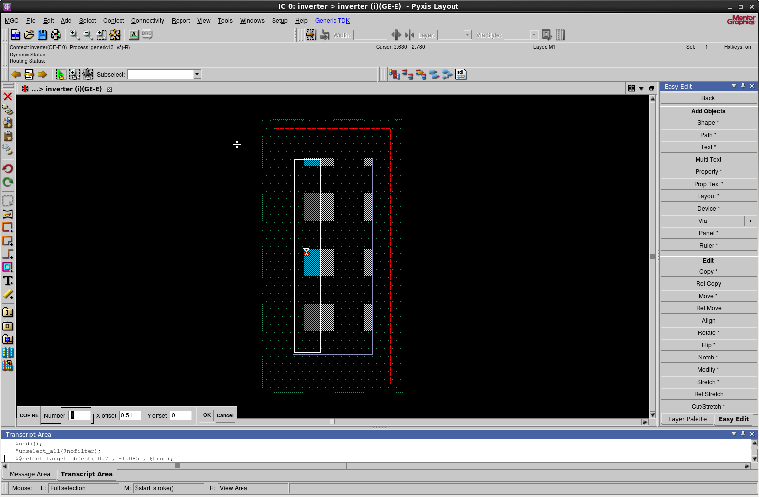
The next step is to create the contacts on the transistor. We will start by making the first contact.
| Type | CO |
| Width | 0.16 |
| Length | 0.16 |
| Origin X | 0.64 |
| Origin Y | -0.36 |
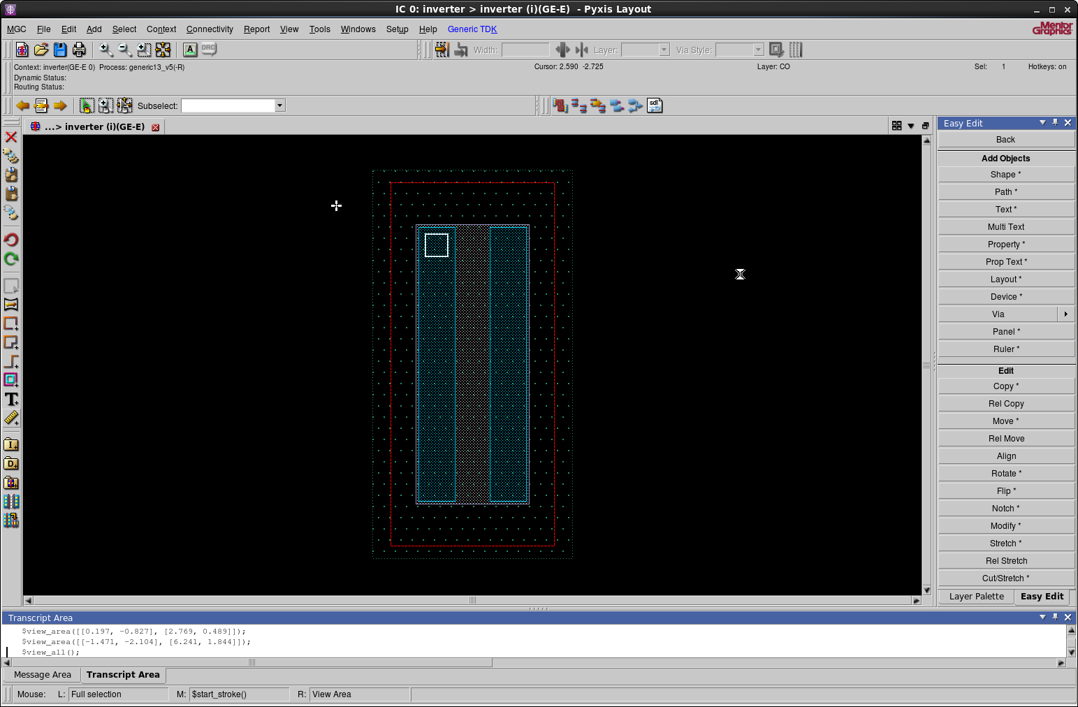
Then relatively copy along y with the correct spacing as shown below.
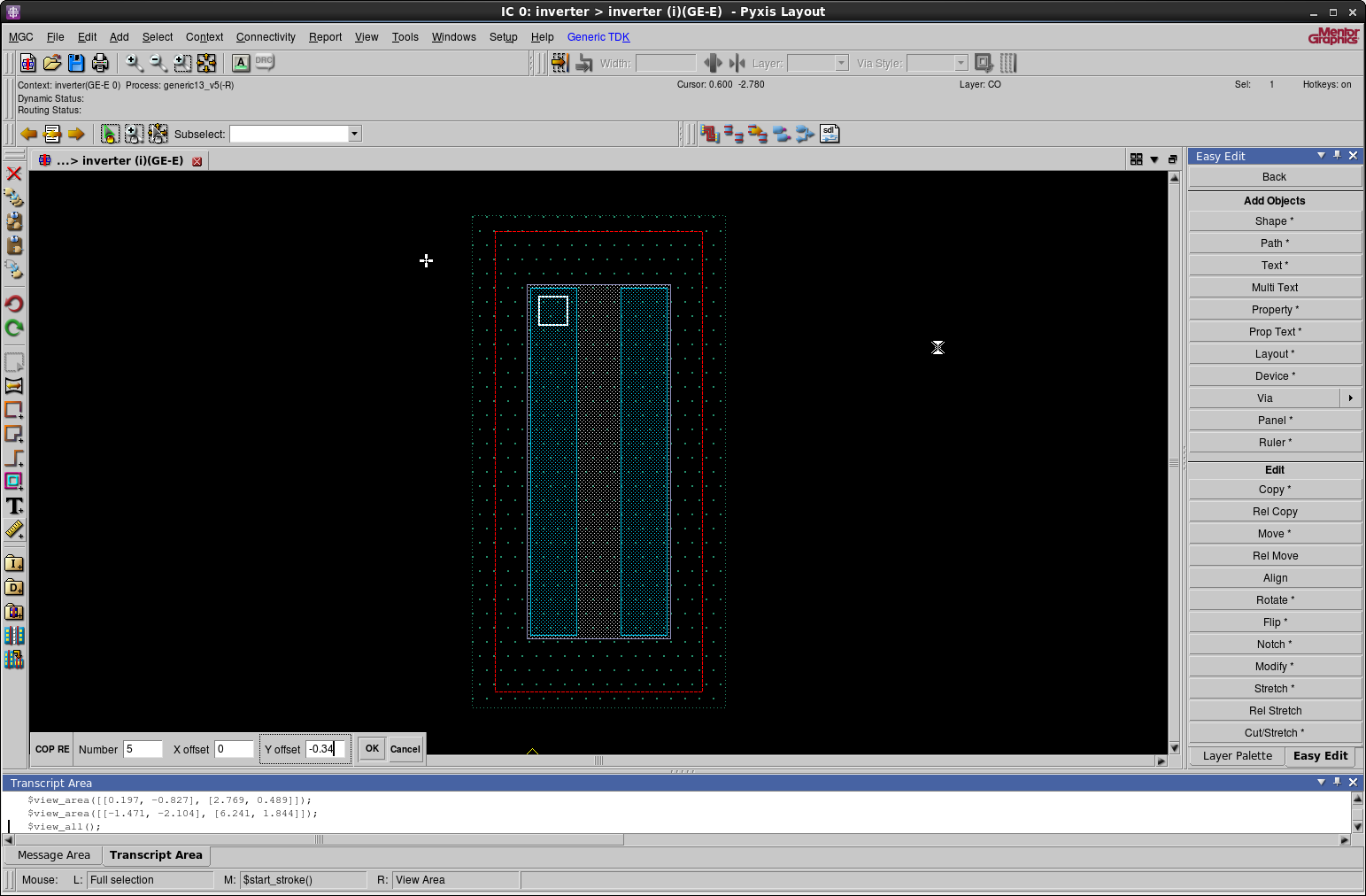
You should now have six contacts on your transistor.
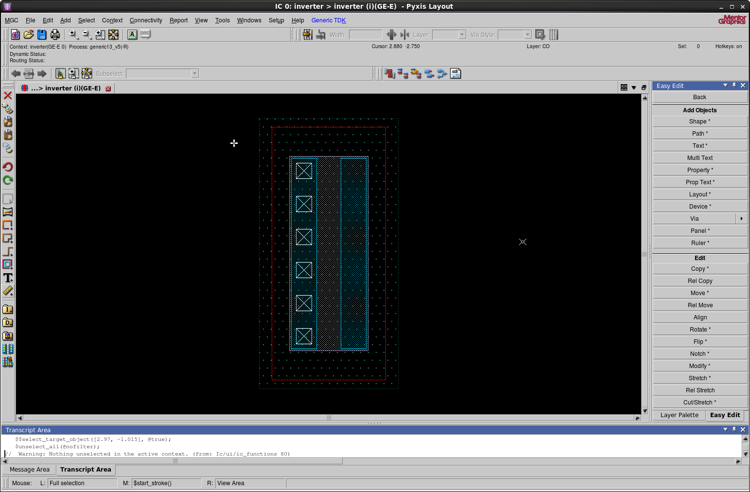
Select one of the contacts, hold Shift, and select the rest of the
contacts. Then relatively copy along x.
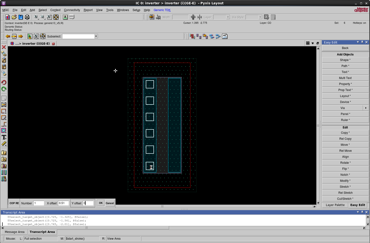
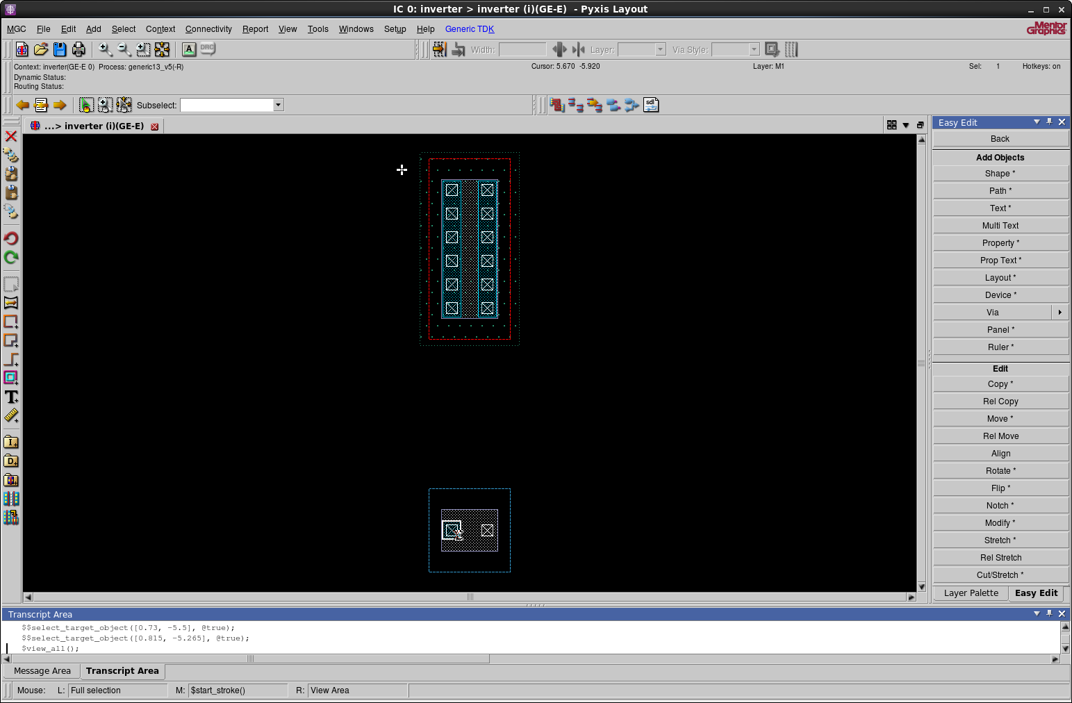
We've successfully created a PMOS transistor. The final layout should look like the one shown below.

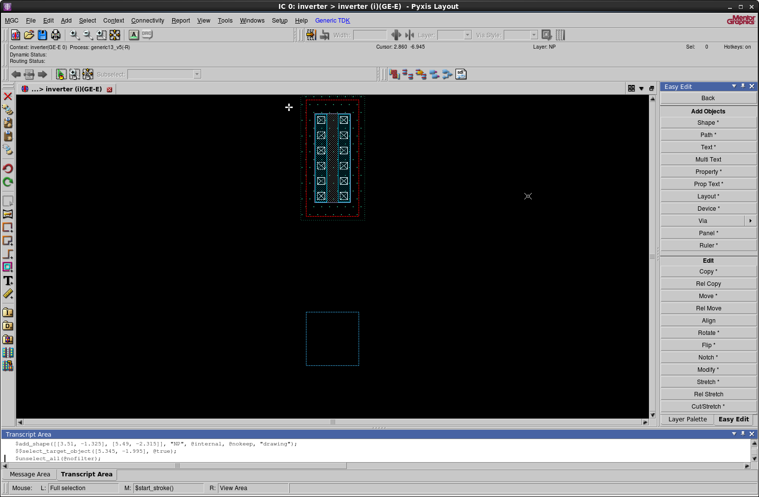
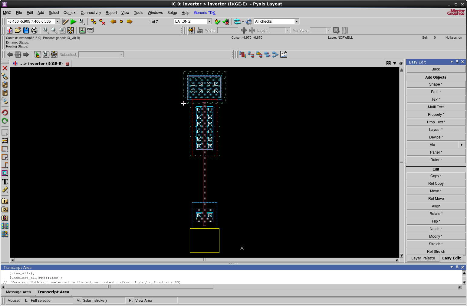
Creating the NMOS transistor
| Type | NP |
| Width | 1.17 |
| Height | 1.2 |
| Origin X | 0.39 |
| Origin Y | -5.78 |
| Type | OD |
| Width | 0.81 |
| Height | 0.6 |
| Origin X | 0.57 |
| Origin Y | -5.48 |
| Type | CO |
| Width | 0.16 |
| Height | 0.16 |
| Origin X | 0.64 |
| Origin Y | -5.26 |
Relatively copy along x with an offset of 0.51 μm.

| Type | M1 |
| Width | 0.26 |
| Height | 0.26 |
| Origin X | 0.59 |
| Origin Y | -5.31 |
Relatively copy along x with offset of 0.51 μm.

| Type | POLYG |
| Width | 0.13 |
| Height | 5.71 |
| Origin X | 0.91 |
| Origin Y | -5.66 |
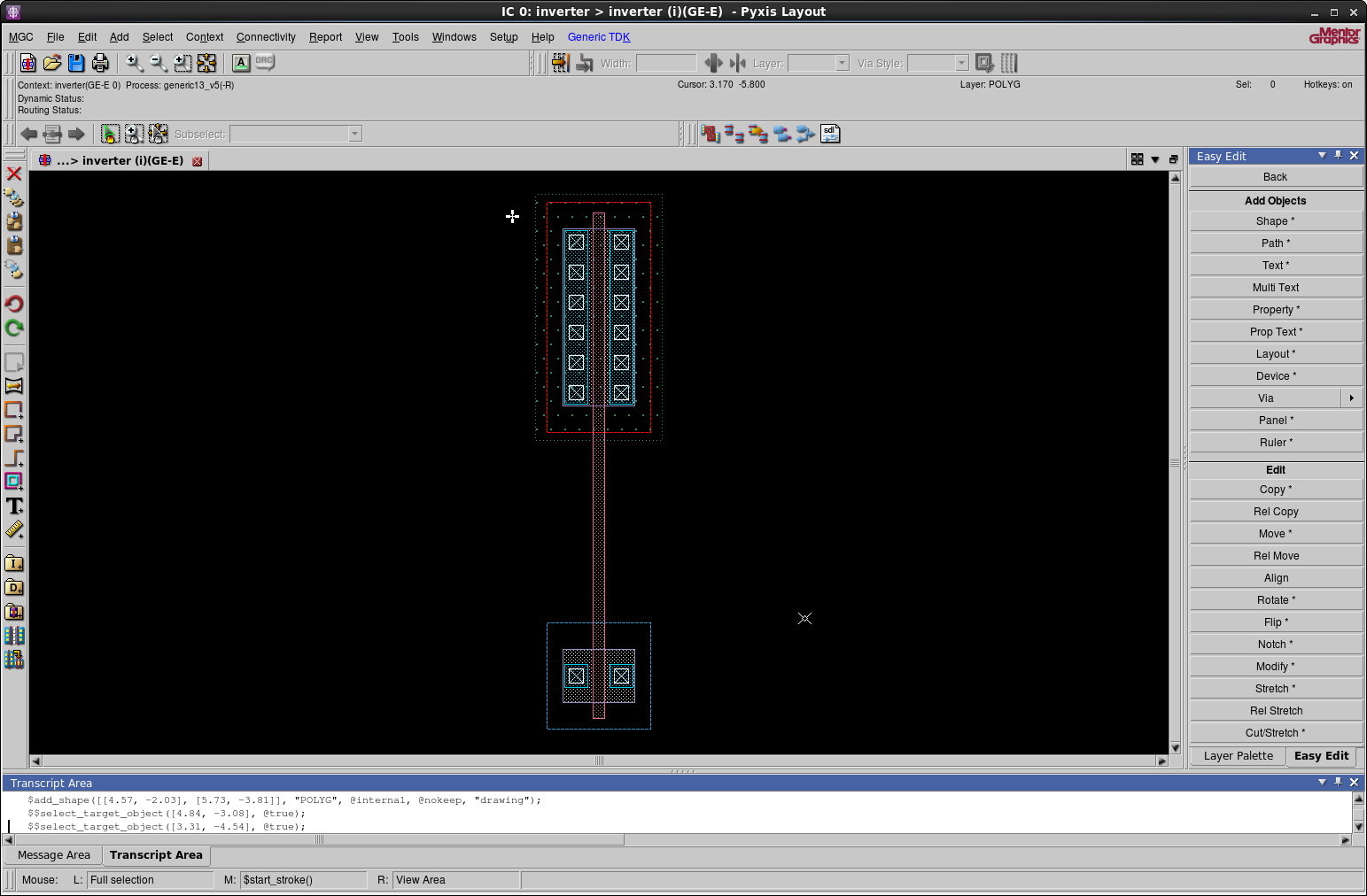
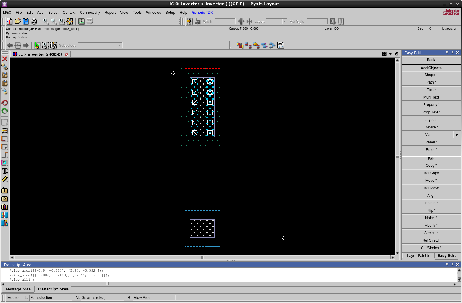
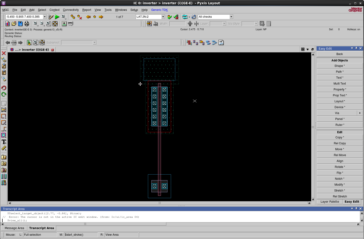
At this point it might be beneficial to check the structure that we have completed thus far. This can be accomplished by running a Design Rule Check (DRC). The DRC will warn you of any shapes too close together or any partial connections.
Navigate to Tools > Calibre > Run DRC. You don't need to change anything
in Calibre Interactive just press Run DRC.
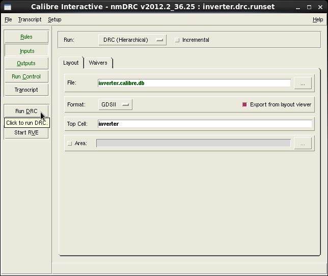
Check at the end of DRC Summary Report.You should get a total of seven warnings. All but one will be fixed by the
end of this tutorial.
Remark: It is of importance that you do frequent DRC checks during the design of a circuit. That way, you avoid having to make extensive changes as a result of not having enough room to move things around to eliminate a design rule violation.
Creating the Positive Supply Voltage (

| Type | NW |
| Width | 1.95 |
| Height | 1.48 |
| Origin X | 0 |
| Origin Y | 0 |

| Type | NP |
| Width | 1.59 |
| Height | 1.12 |
| Origin X | 0.18 |
| Origin Y | 0.18 |
| Type | OD |
| Width | 1.47 |
| Height | 1 |
| Origin X | 0.24 |
| Origin Y | 0.24 |
| Type | M1 |
| Width | 1.43 |
| Height | 0.96 |
| Origin X | 0.26 |
| Origin Y | 0.26 |

Create the contacts of 

| Type | CO |
| Width | 0.16 |
| Height | 0.16 |
| Origin X | 0.355 |
| Origin Y | 0.84 |

Relatively copy along y with an offset of -0.36 μm.

Select both the contacts by holding Shift + Left Click. Relatively copy
along x with an offset of 0.36 μm. Set the number of copies to three.
Run DRC as before. The number of total warnings should have dropped to five.
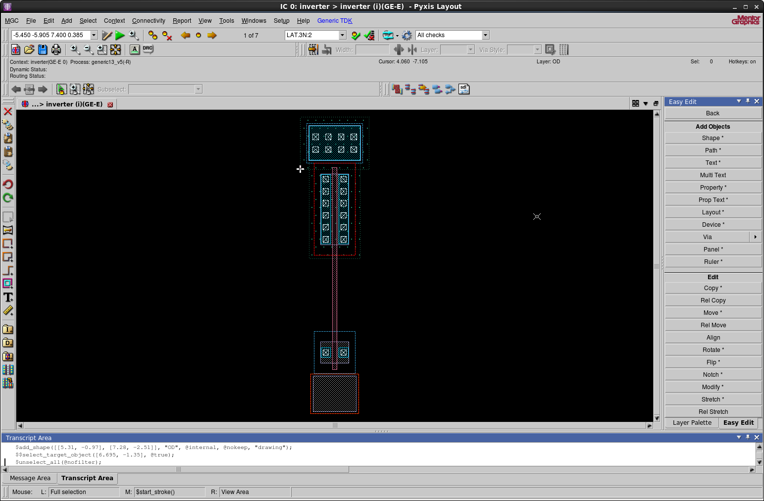
Creating the Reference Node (Ground)
| Type | NOPWELL |
| Width | 1.35 |
| Height | 1.12 |
| Origin X | 0.3 |
| Origin Y | -6.91 |
| Type | PP |
| Width | 1.35 |
| Height | 1.12 |
| Origin X | 0.3 |
| Origin Y | -6.91 |

| Type | OD |
| Width | 1.23 |
| Height | 1 |
| Origin X | 0.36 |
| Origin Y | -6.85 |
| Type | M1 |
| Width | 1.19 |
| Height | 0.955 |
| Origin X | 0.38 |
| Origin Y | -6.83 |
| Type | CO |
| Width | 0.16 |
| Height | 0.16 |
| Origin X | 0.535 |
| Origin Y | -6.25 |

Relatively copy along y with an offset of -0.36 μm.

Select both the contacts by holding Shift + Left Click. Relatively copy
along x with an offset of 0.36 μm. Set the number of copies to two.

Run DRC once again. Your number of total warnings should have reduced to three.
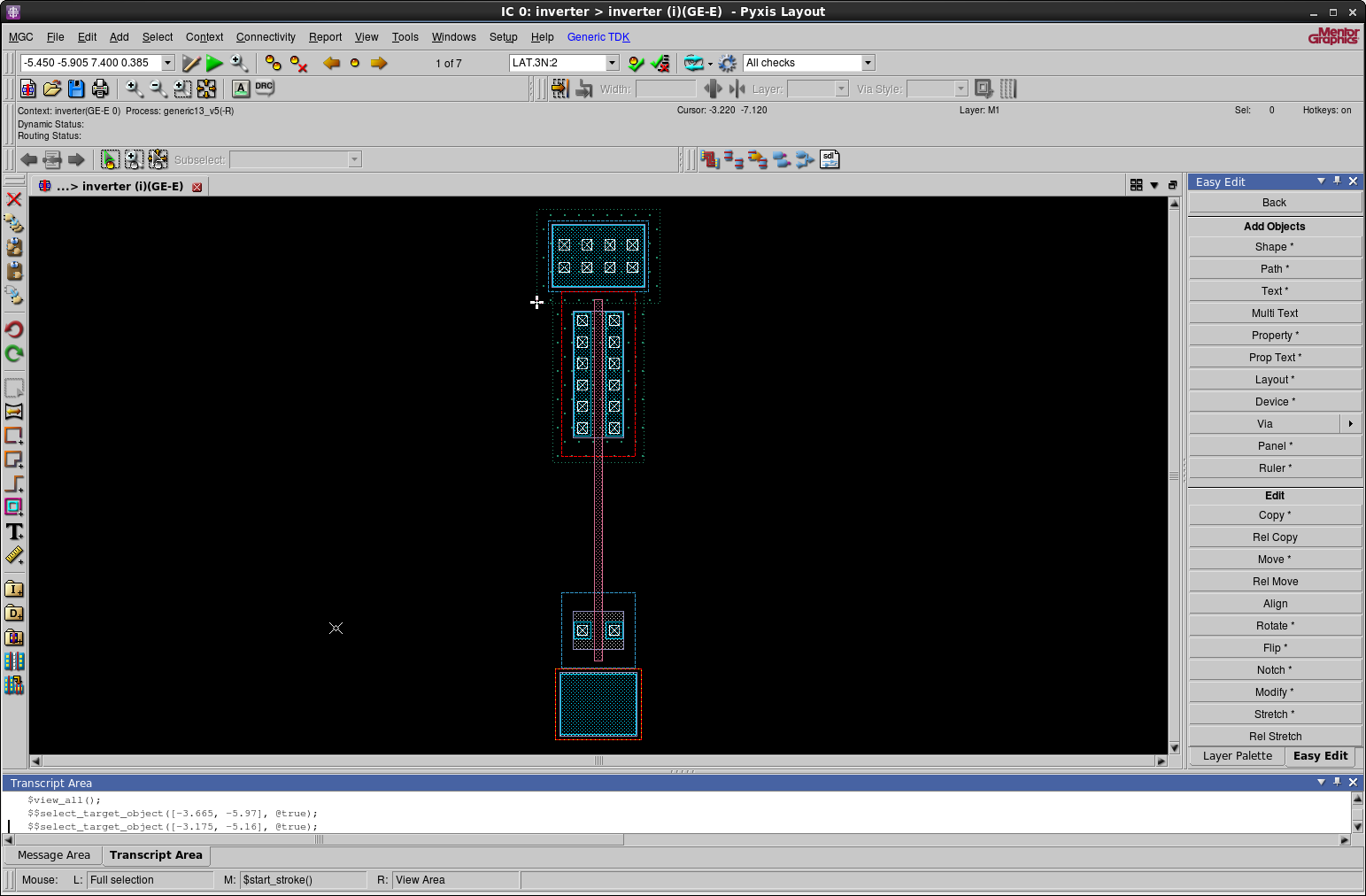
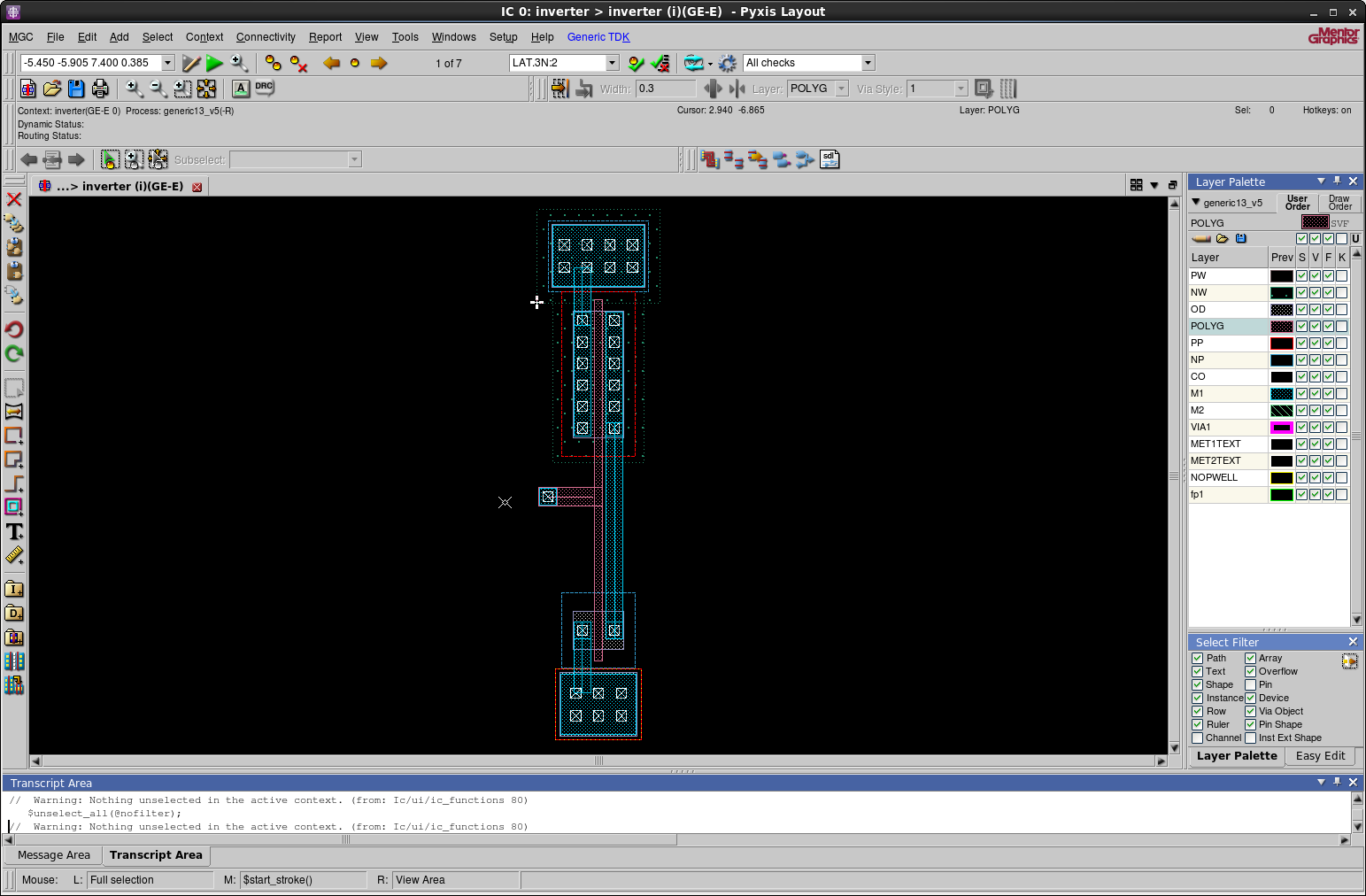
Wire the Circuit
Since this cell is to be used in a much larger circuit, it needs to have
points where the connections can be made (e.g., input, output,
Connect ground to the NMOS transistor by selecting Metal 1 (M1) and
navigating to Add > Path. Press q and change the path width to 0.26
μm. This will stop the Add Path function so call it again. It should now
be the correct size. Start from the left contact of the NMOS and lay the path towards
the Metal 1 of the ground node. The result should look like the one shown
below.
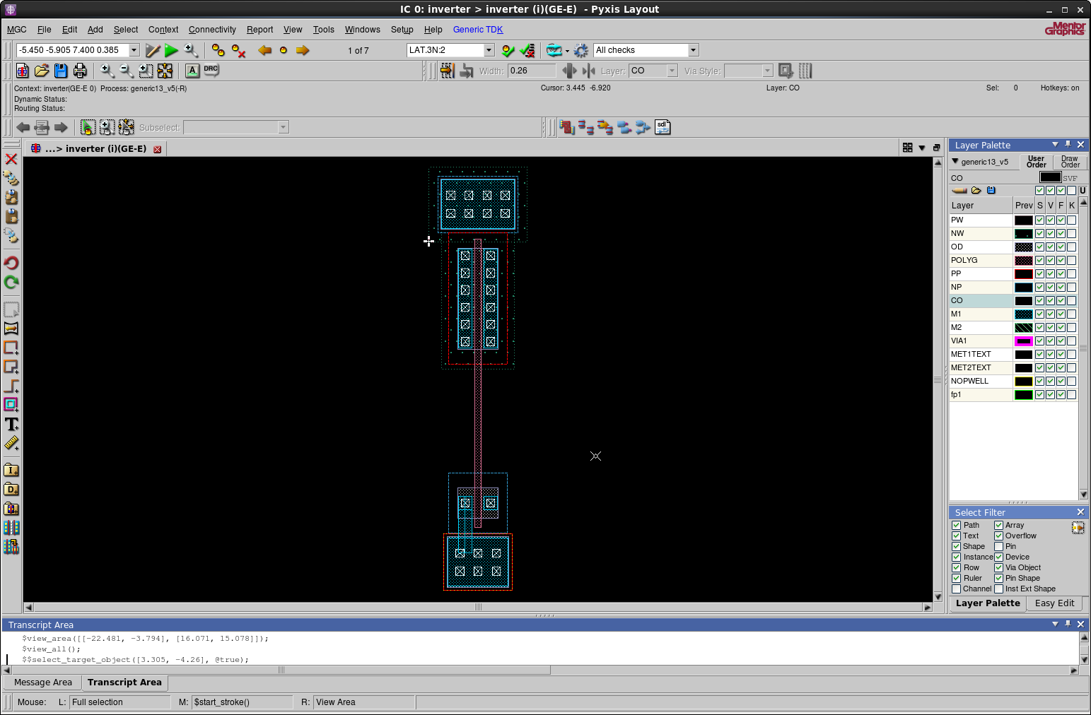
Similarly connect the PMOS transistor to
Wire the NMOS transistor with the PMOS transistor.
Create a path for the input. You will need to connect POLYG to METAL
1. Call the Add Path function and the press o. This component will
allow for that "transition". Place that component at origin x equal to 0.18
and at origin y equal to -3.065.

Lay a path from the POLYG to the middle of the component. You can achieve
that by choosing POLYG in the Layer Palette and changing the path width to
0.3 μm. The result should look like the one below.
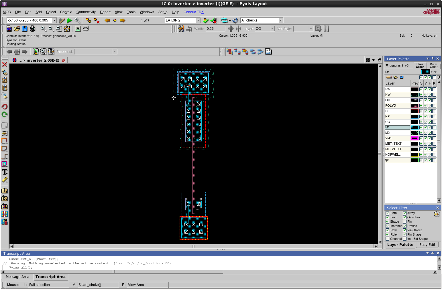
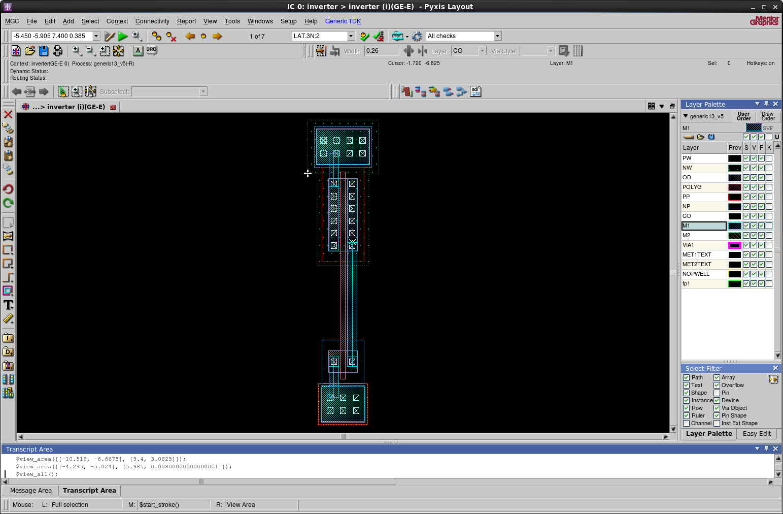
Lay a Metal 1 path, of width 0.26 μm, as shown below to represent the input.

Lastly create a Metal 1 path for the output as shown below.
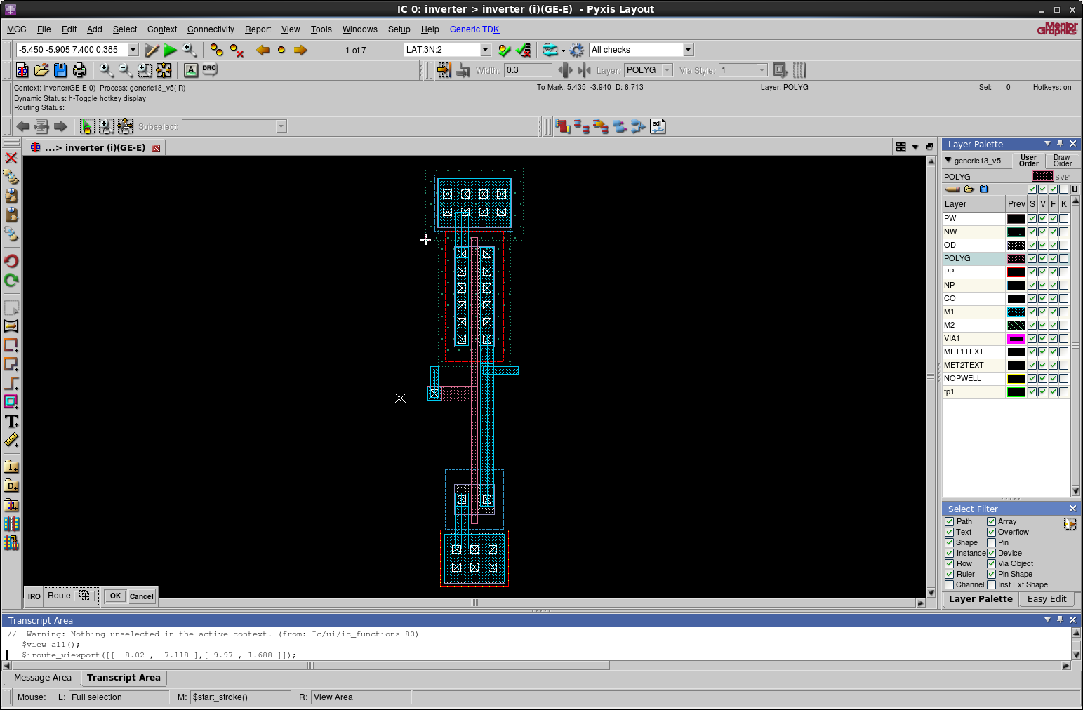
Run DRC. You should now only have one warning left. It states that the area
coverage of POLYG is less than 14%. This is not a serious error, but it's
part of the Generic 0.13 micron process that we are using.
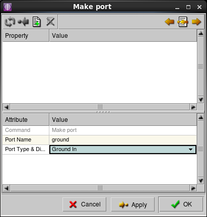
Create Ports
Choose the Metal 1 layer of the reference node and navigate to
Connectivity > Port > Make Port:. Name the port ground and change the
port type to Ground In. Press OK.
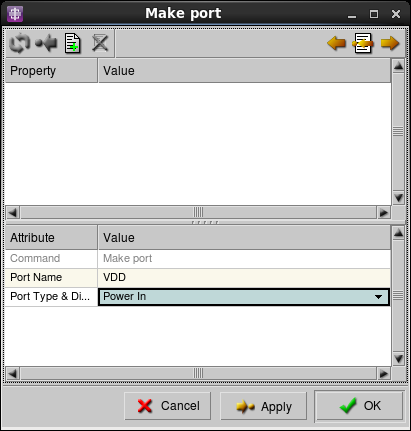
Choose the Metal 1 layer of the VDD and change the port type to Power In. Press OK.
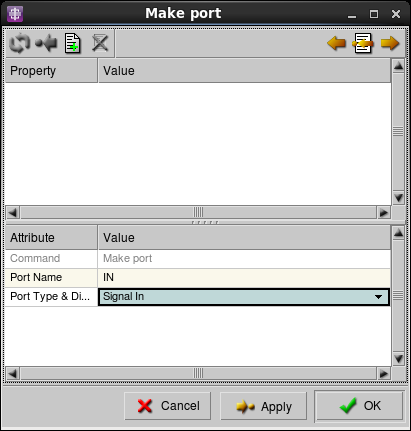
Choose the path dedicated to the input node and make a port. Name the port IN and
change the port type to Signal In
Choose the path dedicated to the output node and make a port. Name the port
OUT and change the port type to Signal Out.

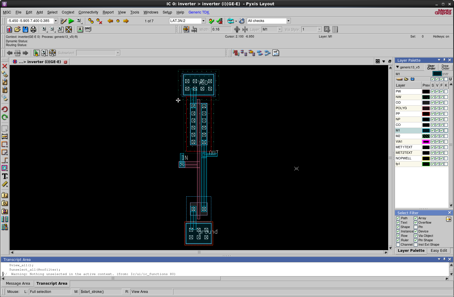
Finally navigate to Add > Text on Ports.... As the name implies this will
add text that will indicate the input, output, OK. The resulting layout should look
like the one below.
Perform a DRC to make sure we didn't introduce any warnings during the above procedure.
Layout vs. Schematic (LVS) Check
It's sometimes beneficial to compare the schematic implementation of a
circuit against the layout implementation of the same circuit. In Tutorial
1 we created a schematic of an inverter. Henceforth, the two will be
compared to evaluate the correctness of the above design.
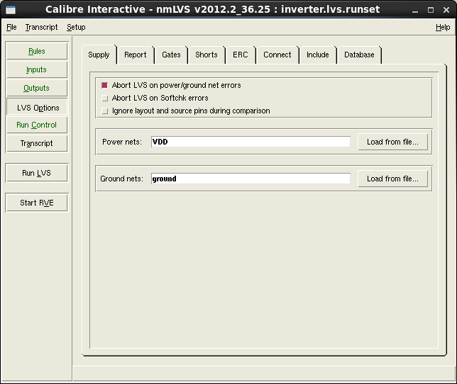
Navigate to Tools > Calibre > Run LVS.
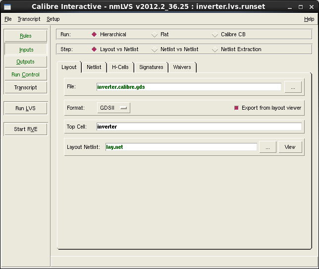
Click on the Netlist Tab and change the Top Cell to Tutorial_1.
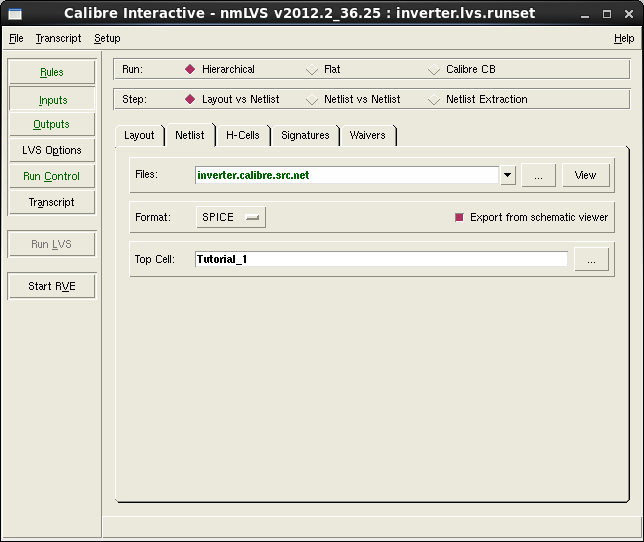
Then navigate to Setup > LVS Options and add
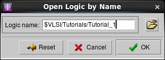
Since our schematic exists under the Tutorial_1 you will be prompted to
locate the path.
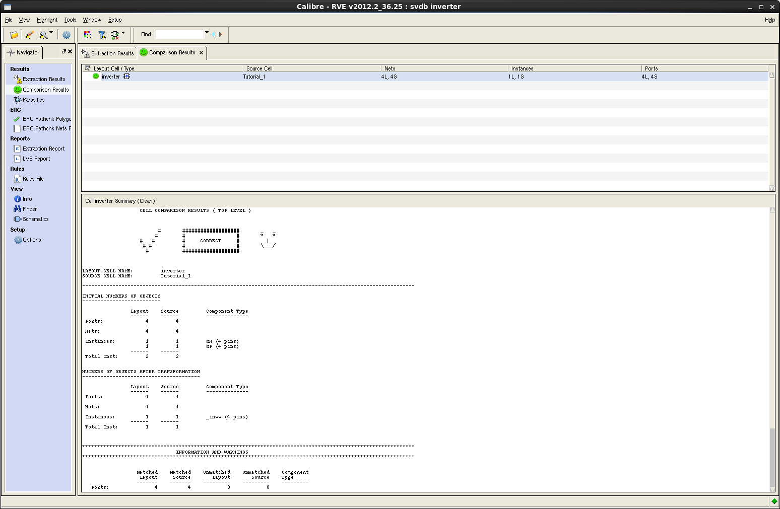
If your design is correct you will get the below result.
Finally, be sure to save your cell then exit Pyxis Layout.